Micromechanics & Nanomechanics: Difference between revisions
Oluschinski (talk | contribs) Created page with "{{Language_sel|LANG=ger|ARTIKEL=Mikro- und Nanomechanik}} {{PSM_Infobox}} <span style="font-size:1.2em;font-weight:bold;">Micromechanics & Nanomechanics (''Author: Prof. Dr. G. H. Michler'')</span> __FORCETOC__ ==Introduction== The various applications of plastics require the full utilization of a material's property potential. However, the mechanical properties are particularly important for almost all applications, as the actual application properties..." |
(No difference)
|
Latest revision as of 13:09, 3 December 2025
| A service provided by |
|---|

|
| Polymer Service GmbH Merseburg |
| Tel.: +49 3461 30889-50 E-Mail: info@psm-merseburg.de Web: https://www.psm-merseburg.de |
| Our further education offers: https://www.psm-merseburg.de/weiterbildung |
| PSM on Wikipedia: https://de.wikipedia.org/wiki/Polymer Service Merseburg |
Micromechanics & Nanomechanics (Author: Prof. Dr. G. H. Michler)
Introduction
The various applications of plastics require the full utilization of a material's property potential. However, the mechanical properties are particularly important for almost all applications, as the actual application properties cannot be utilized if the material breaks prematurely due to insufficient strength or lack of toughness. In order to be able to significantly rule out fracture as one of the most frequent causes of failure, there are increased demands on the development of measurement and testing methods, e.g. in-situ techniques, and on the evaluation with material science-based parameters. The precise determination of mechanical behaviour therefore plays an important role in materials science. Micro- and nanomechanical analyses, known as micro- and nanomechanics, are used to gain a better understanding of material behaviour and to specifically improve material properties. Some examples are presented below.
However, the term micromechanics is also used in two other senses, for the manufacture of miniaturized components or devices and for micromachining electronic components, but this will not be discussed here [1, 2].
Micromechanical analyses
The various mechanical tests are based on standardized test specimens. This generally determines the macroscopic, average material behaviour. Local effects such as those caused by stress concentrations, thermo-mechanical loads, production-related residual stresses or material inhomogeneities are thus masked. In addition, the trend towards miniaturization of components (microsystems) means that local defects have a greater impact. For this reason, there has already been a transition from macro to micro testing technology in the past. Furthermore, standard test specimens are very material-intensive and are therefore often not available for the development of new, optimized material systems.
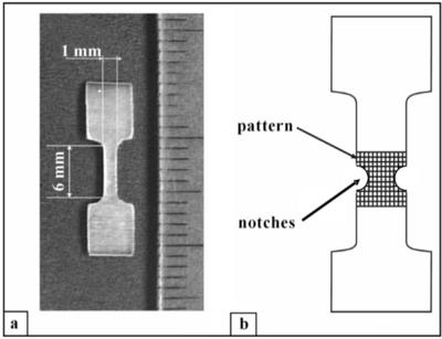
| Fig. 1: | Special test specimen shape for micro tests a) View of the entire test specimen, b) Notched test specimen with vapor-deposited silver pattern |
A special miniaturized test specimen shape is shown in Fig. 1, which can also be used for observations in optical light microscopes, scanning electron microscopes (SEM) and atomic force microscopes (AFM) (see below). The vapor-deposited silver dots make it possible to detect changes in local deformation by measuring the distance between the dots. They are also helpful to localize the same material site during deformation at higher magnifications in the optical microscope or SEM.
Microscopic techniques
A comprehensive understanding of micromechanical processes must be accompanied by a detailed investigation of the morphology and in particular those structural parameters that significantly determine or influence the mechanical properties. Microscopic methods can capture the morphology and the micromechanical properties at the same material site and therefore provide a direct way to establish structure–property relationships.
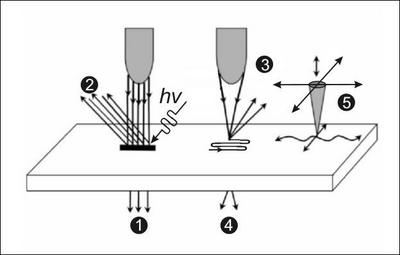
This is based on the different techniques of light and electron microscopy, which are generally classified in Fig. 2 according to whether an image is obtained by irradiation as with a “lamp” or by scanning the surface as with a “finger” or a “needle”.
| Fig. 2: | Schematic representation of the most important types of microscopy (1 - 5 see text) |
The most important variants of microscopic imaging techniques are:
- Transillumination of a probe using light in conventional light microscopy in the transmission mode or with electrons in the transmission electron microscope (TEM). The electron beam in the TEM is generated in a high vacuum, and several electron microscope lenses connected in series produce a magnified image of the object. This requires ultra-thin probes in the range of 0.1 to a few µm.
- Backscattering of a beam at the surface of a probe in the reflected light microscope or in the electron reflecting microscope. By irradiating the probe with electrons, ions or ultraviolet light (indicated by hν), the sample itself is excited to emit electrons – in the emission electron microscope (PEEM). Compact probes can be examined.
- A focused electron beam is scanned over the probe and generates secondary and backscattered electrons in the probe through elastic and inelastic scattering processes (scanning electron microscope – SEM). If the probe chamber is not under the usual high vacuum, but under reduced vacuum, materials can also be examined in their natural environment – in the ambient SEM or Environmental Scanning Electron Microscope (ESEM).
- The focused electron beam scans over the (sufficiently thin) probe and penetrates it; a detector below the probe catches the electrons – scanning transmission electron microscope.
- A very thin tip is scanned over the probe and interacts with the probe due to various physical properties – for conductive probes in scanning tunneling microscopy and for insulating materials in atomic force microscopy, general scanning sensor microscopy. No vacuum is required and surfaces of compact probes can be examined. This technique is not an actual electron microscopy method, but is often used in addition to these.
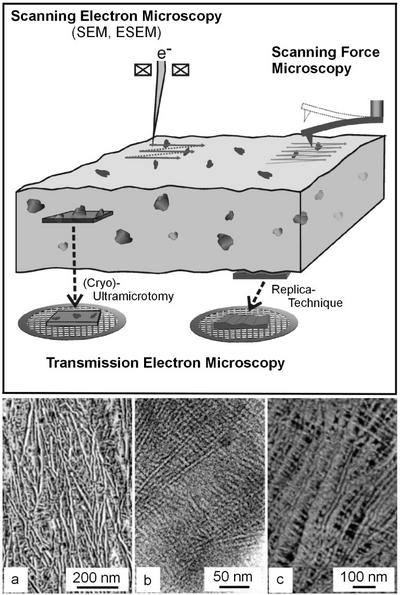
A schematic overview of these different techniques with typical application conditions on a compact material is shown in Fig. 3. A compact overview of these electron microscopic techniques can be found in [3, 4].
| Fig. 3: | Schematic overview of the various microscopic techniques for the examination of compact materials: investigation of surfaces using scanning electron microscopy and atomic force microscopy; surfaces can also be captured using the replica technique, investigation of internal material structures using transmission electron microscopy on (ultra)thin probes (produced e.g. using (cryo-) ultramicrotomy) |
Micromechanical in-situ investigations
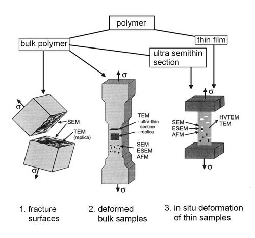
Using the electron microscopy techniques mentioned in Figures 2 and 3, micromechanical processes can also be recorded in addition to the detailed investigation of the morphology. For this purpose, the materials are mechanically loaded in various ways – see Fig. 4 (details in [3]):
| Fig. 4: | Overview of electron microscopy techniques for investigating micromechanical processes in compact materials |
- Fracture surfaces of compact bodies loaded to fracture are analysed in the scanning electron microscope (SEM, or with an older technique of impression production (replica) in the TEM at higher magnification).
- Compact bodies are deformed and surface structures from the deformation areas are examined in detail in the SEM, ESEM, AFM or after preparation of thin sections from the interior in the TEM.
- Probes are stretched directly in a microscope and observed together with the local morphology. Compact probes are analysed in the SEM, ESEM or ADFM, ultra-thin samples (e.g. ultramicrotome sections) in the TEM and semi-thick probes (which better reflect the properties of the compact material) in the high-voltage TEM.
Bending tests are carried out on compact test specimens on which surface structures are investigated in the SEM and internal structural details on thin sections (prepared from the loaded areas by means of ultramicrotomy) in the TEM at higher magnification.
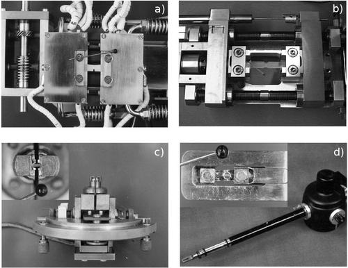
Various stretching devices are commercially available for carrying out the micromechanical tests, some of which are shown in Fig. 5 and some of which also allow loads to be applied over a wide temperature range.
| Fig. 5: | Commercially available in-situ stretching devices for the different microscope types |
a) Stretching stage for SEM from Oxford Instruments, temperature range during stretching from -180 oC to 200 oC; compact and semi-thick probes b) Stretching device for SEM and AFM from Kammrath & Weiss, probe thickness 10 µm ... 5 mm
c) Stretching stage for a 100 kV-HEM (JEOL), probe thickness 100 nm ... 5 µm
d) Stretching lancet for TEM (Gatan), temperature range -180 oC …120 oC, probes thickness 100 nm ... 0.5 µm
In addition, there are also interesting in-house developments in various research institutions to enable special testing requirements ( bending tests, high-temperature elongation, elongation under electric/magnetic fields and others).
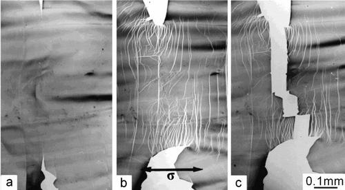
As an example of an in-situ deformation test in a TEM (1,000 kV high-voltage electron microscope, HEM), Figure 6 shows a sequence of three images of increasing elongation of an approx. 0.5 µm thick polystyrene sample ( abbreviation: PS; ultramicrotome semithin section) at low magnification. The formation of local deformation zones (crazes – Fig. 6b) starts at two artificially applied notches. The crazes are up to 100 µm long and appear as bright bands due to their internal structure of micro-holes and fibrils. After a small additional deformation, the largest crack ruptures and initiates a brittle fracture (Fig. 6c).
| Fig. 6: | In-situ deformation of a 0.5 µm thick PS specimen (semi-thin section) in a 1,000 kV HEM; deformation direction see arrow σ |
a) with artificial cracks before stretching
b) after elongation of approx. 10 % with local deformation bands (bright)
c) after crack propagation and brittle fracture
See also
References
| [1] | Michler, G. H.: Werkstoffwissenschaft und Kunststoffe. Schriften der Sudetendeutschen Akademie der Wissenschaften und Künste. Band 43, Forschungsbeiträge der Naturwissenschaftlichen Klasse, Munich (2024) 27–58 (see AMK-Library under F 33) |
| [2] | Michler, G. H.: Mechanik – Mikromechanik – Nanomechanik. Vom Eigenschaftsverstehen zur Eigenschaftsverbesserung. SpringerSpektrum (2024), ISBN 978-3-662-66965-5; e-book: ISBN978-3-66966-2; https://doi.org/10.1007/978-3-662-66966-2; see AMK-Library under F 34 |
| [3] | Michler, G. H.: Electron Microscopy of Polymers. Springer Berlin, Heidelberg (2008); ISBN 978-3-540-36350-7; see AMK-Library under F 1 |
| [4] | Michler, G. H.: Kompakte Einführung in die Elektronenmikroskopie: Techniken, Stand, Anwendungen, Perspektiven. Springer Spektrum – Essentials (2019); see AMK-Library under F 21 |
| [5] | Michler, G. H.; Balta-Calleja, F. J.: Nano- and Micromechanics of Polymers: Structure Modification and Improvements of Properties. Carl Hanser München (2012); ISBN 978-3-446-42767-9; see AMK-Library under F 13 |
| [6] | Michler, G. H.: Kunststoff-Mikromechanik: Morphologie, Deformations- und Bruchmechanismen; Carl Hanser München (1992); ISBN 3-446-17068-5, see AMK-Library under F 4 |
| [7] | Michler, G. H.: Atlas of Polymer Structures: Morphology, Deformation and Fracture Structures, Carl Hanser München (2016); ISBN 978-1-56990-557-9 E-Book ISBN 978-1-56990-558-6, see AMK-Library under F 14 |
Weblinks
- Wikipedia – Die freie Enzyklopädie: Mikromechanik; https://de.wikipedia.org/wiki/Mikromechanik und Nanowissenschaften, https://de.wikipedia.org/wiki/Nanowissenschaften
- Nanomechanik: https://www.ww1.tf.fau.de/forschung/nanomechanik/
- Universität Kassel: Lehrveranstaltung Mikro- und Nanomechanik; https://www.uni-kassel.de/maschinenbau/institute/werkstofftechnik/fachgebiete/mechanisches-verhalten-von-werkstoffen/studium-lehre/mikro-und-nanomechanik

